Laser Drilling
ESI UV Laser
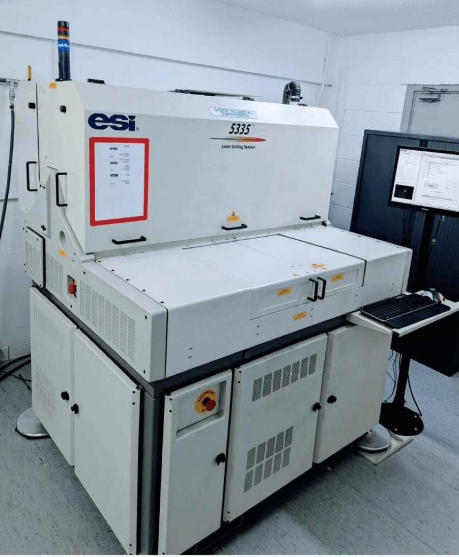
ESI UV Laser is a high-precision UV laser processing system used for HDI PCB, package substrate, and advanced circuit board manufacturing.
Specifications
- Manufacturer
- ESI
- Model
- UV Laser
- Working Area
- PCB Panel Support
- Spindle
- -
- Speed
- High-speed UV laser processing
- Power
- UV Laser
- Voltage
- Factory Spec
- Application
- HDI PCB, Package Substrate, Fine Pattern
Detailed Description
Overview
ESI UV Laser is a high-precision laser processing system designed for advanced PCB and semiconductor package substrate manufacturing.
The short wavelength of UV laser technology minimizes thermal impact while providing excellent precision for micro via drilling and fine pattern processing.
It is widely used in smartphone PCB, server PCB, semiconductor package substrate, and high-density circuit board production lines.
Key Features
- High-precision UV laser processing
- Suitable for micro via drilling
- Fine pattern processing capability
- Minimal thermal damage
- Supports advanced HDI PCB production
- Suitable for semiconductor package substrates
- Excellent processing quality and productivity
Applications
This system can be used for HDI PCB, build-up PCB, semiconductor package substrate, smartphone PCB, server PCB, and advanced circuit board manufacturing processes.